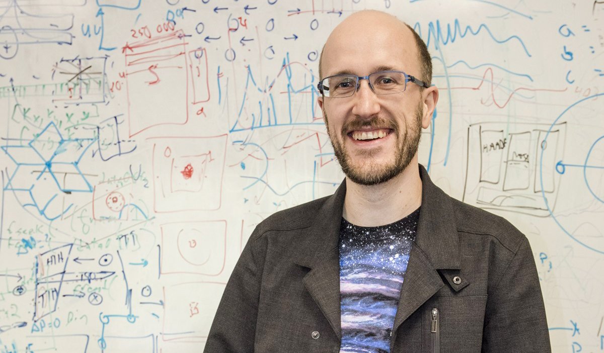
Colin Ophus: “A 4D STEM Detector Should Provide the Full Picture of Beam-Specimen Interaction”

A 20-minute read
4D STEM is on the rise in the electron microscopy community. We could not resist discussing this exciting family of techniques with one of the leading experts on the subject.
Dr. Colin Ophus is from the National Center for Electron Microscopy (NCEM), which is part of the Molecular Foundry at Lawrence Berkeley National Laboratory. From detector requirements to machine learning, our discussion had an interesting twist.
DECTRIS: What led you to the NCEM at Lawrence Berkeley National Laboratory?
Dr. Colin Ophus, Staff Scientist at the NCEM: I was convinced that I would become an engineer, so I started my degree in electrical engineering and later transferred to engineering physics. Little did I know that my career was going to take such an unexpected trajectory.
During my studies, I had to complete an end-of-semester project; that led to a summer internship at my professor’s laboratory, where I got hooked on scientific research. I really appreciated the extreme freedom in tackling problems in science, and I ended up doing a Ph.D. in Materials Engineering in that lab.
Back then, TEM (Transmission Electron Microscopy) was already gaining momentum in Materials Science research, and our lab had connections at the NCEM. We submitted a user proposal, and I found myself flying down to California for months at a time to use the NCEM’s microscopes. Even today, I cannot think of a better place to learn TEM. I was lucky enough to be trained by Velimir Radmilović (Mimo). He and other scientists at the facility taught me so much about electron microscopy!
When I got a postdoc scholarship, I was at a crossroads: I had to choose between pursuing my interest in computational work or my interest in TEM. Luckily, I found a way to do both. Co-supervised by Mark Asta from UC Berkeley, I studied density functional theory while continuing my work with Mimo. Finally, after my postdoc, I was offered the position of a computational scientist at the NCEM. It snowballed from there, and eventually, I became a staff scientist with my own group that is focused on computational microscopy. I am very happy with how things turned out: there are few facilities in the world that perform research like ours.
Escape Room, Ophus Style
DECTRIS: If you were to highlight one of your scientific accomplishments, which one would you choose, and why?
Colin: I was fortunate to work with so many amazing collaborators; it is difficult to pick one accomplishment over another. I guess my personal highlight is the PRISM algorithm for STEM (Scanning Transmission Electron Microscopy) simulation, because it is the only single-author publication I have ever had. I remember I was struggling to simulate a large field-of-view STEM image, as it involved over a million independent simulations. In an attempt to find a better solution, I literally locked myself in a room with a pen and paper. After several days, I hit upon a couple of ideas for how to improve the process.
Once the code was implemented, I could perform STEM image simulations a thousand times faster than before. But the biggest recognition came when other researchers, like Hamish Brown (from the University of Melbourne), or Thomas Susi and Jacob Madsen (from the University of Vienna), picked up the idea and implemented it in their own software. This was proof that my algorithm was useful!
DECTRIS: What is your opinion on the recent trends in (S)TEM?
Colin: I might be biased, seeing as I am a computational scientist with a weakness for data, but I see the most potential in improving data acquisition and data quality in 4D STEM.
Direct electron detectors have improved quantum efficiency such that they can operate by counting individual electrons, at speeds that are fast enough to operate at the native speed of a STEM experiment. These recent advancements in hardware – in particular, in detector technology – enable us to collect a lot more, and better, data.
Five Beamlines in One Instrument
Another trend that I find very exciting is multimodal experiments. Nowadays, we typically collect only a few channels: such as the forward diffraction pattern, scattered X-rays, backscattered electrons, a spectroscopic scan of inelastic energy losses, or other channels such as cathodoluminescence. However, STEMs are the perfect multimodal instruments – we could collect all of these data streams at once!
It is the equivalent of five beamlines in a synchrotron, merged into one instrument. These multimodal experiments will generate a statistically significant number of diffraction images or spectra, and also feed computational models with enough data to produce robust results.
It is great to see how the scientific community is moving away from the old convention of recording one or two publication-worthy images, and instead starting to appreciate the value of collecting large data sets to better understand the bigger picture. Even more so, with computer and detector technology improving every year.
DECTRIS: Speaking of detectors, what role will they play in the development of STEM – 4D STEM, in particular?
Colin: My expectation of a 4D STEM detector is that it provides the full picture of beam-specimen interaction. Whether you are in Life Science or Materials Science, the ultimate goal is to collect every electron while maintaining good time resolution.
Compare our fields to particle physics: for years, those scientists have been collecting all of the scattered, generated, or annihilated particle trajectories and using them to reconstruct what happened inside the material. We want to do the same! Luckily, we already have the technology that allows us to capture the position and momentum of all scattered electrons, with sufficient speed to track relevant physical processes.
Then, of course, a detector can be configured to fit the requirements of an experiment. There are products out there that allow us to balance out different aspects, such as time for spatial resolution, or the number of pixels versus time resolution. With our detector development at the NCEM, we are working on reaching 100,000 frames per second. At this speed, collecting individual electrons should be quite easy – but speed should not come at the expense of the high dynamic range or noise-free readout. Commercial detectors are approaching this point, where we will be able to catch every electron over the whole scattering range at the relevant timeframes.
One Platform to Rule Them All
DECTRIS: If you had one wish to express to hardware manufacturers, what would it be?
Colin: Definitely, better detector integration into TEM hardware and software: a centralized, open-control platform. In 4D STEM, for example, I need my detector to be synchronized to the STEM coils and be able to blank the beam. There are so many experiments that I cannot perform because my detector does not “speak” to the microscope’s lenses, the sample stage, or the rest of the hardware.
This lack of integration and open-source software in TEM, in my view, is the biggest hurdle to improving 4D STEM and other techniques. To overcome it, we opt for internal development of our own detectors – but this comes at the cost of missing out on all the incredible features that detector manufacturers are offering, due to their superior engineering resources.

DECTRIS: What are the most important detector parameters in 4D STEM?
Colin: In 4D STEM, the number-one attribute by far is the speed of the detector. The faster it goes, the more individual electrons it can count. Such detectors offer better quantum efficiency, but they also enable experiments at a native speed, which for STEM imaging is ~1 million probe positions, with pixel dwell times in the range of 1-100 microseconds. We have seen an evolution of fast detectors: from CCD detectors with 10 frames per second, to the first generation of direct electron detectors going up to 1,000 frames per second, and now the second generation operating at 10,000 frames per second.
The next most important parameter depends on the technique. On the one hand, for diffraction experiments such as pattern classification, phase-orientation, strain mapping, and other experiments that rely on the angular resolution of the beam, it would be the number of pixels. For one of our papers on multi-beam electron diffraction, we did 4D STEM with eight beams simultaneously hitting the detector in eight different locations. Such an experiment would not be possible without a significant number of pixels.
On the other hand, techniques like ptychography or phase-contrast imaging require an extreme dynamic range and single-electron sensitivity. In this case, the detector should be able to differentiate between 10,000 electrons and one electron. A good example of this kind of phase-contrast imaging is the work we did with Kwabena Bediako on a kind of dark-field ptychography, which we called 4D STEM Bragg Interferometry.
Fast, Faster, Irrelevant
DECTRIS: Nowadays, detectors get faster and faster. Do you see a point at which going faster would not make sense anymore?
Colin: Absolutely. I believe the best speed range is somewhere between 10,000 and 100,000 frames per second. The lower limit is meant to overcome the drift, while the upper limit is dictated by the native speed of the experiment and realistic beam currents which we can generate, and which the sample can tolerate.
DECTRIS: What is the future of (S)TEM?
Colin: I believe we are approaching an era of big-data experiments. With the advancements in detector and computing technology, the acquired data sets are getting bigger and bigger. I could imagine scanning the entire functional length scale of a solid-state battery with an anode, electrolytic cathode, and capping layers spanning tens of micrometers. An experiment like this might require probing 10,000 x 1,000 sample points, or more. It is an immense amount of data – terabytes of it. But with modern detectors, 4D STEM could tackle such large fields of view.
In addition, I believe STEM should be more automated. The technology is there! Take a look at any synchrotron beamline – it is highly automated. There is room for this in STEM, since a lot of the steps we do – for example, scanning the Regions of Interest (ROI), or performing drift correction – are highly repetitive.
DECTRIS: And where do you see your research going?
Colin: I am personally interested in open-source code for data-centric analysis of 4D STEM. However, I would be remiss not to mention machine learning.
Many current analyses are limited by data quality, and for machine learning the limiting factor is data quantity. However, most of our experiments are ultimately limited by the sample’s quality. This is where machine learning comes in handy, generating accurate results even for messy and thick samples. We have been playing around with it, and the results are astonishing – so, look out for our upcoming publications. I can imagine that our users in the future will analyze their challenging samples with machine-learning methods.
About Colin Ophus, Ph.D.
Colin works primarily on developing methods, algorithms, and code for simulations, analyses, and instrument design in the fields of High-Resolution and Scanning Transmission Electron Microscopy (HRTEM and STEM). He provides computational support to facility users for quantitative analysis of electron micrographs and aims to close the gap between experimentally available data and theoretically accessible systems.
He has also written several software packages to perform image simulations, drift correction, and large data-set visualizations, as well as a substantial number of data-analysis algorithms.
About the National Center for Electron Microscopy (NCEM) at Lawrence Berkeley National Laboratory
The National Center for Electron Microscopy (NCEM) was established in 1983 to maintain a research center at the forefront of electron-optical characterization of materials, with state-of-the-art instrumentation and expertise. It is part of the Molecular Foundry user facility, which is open to proposal submissions from both the industry and academia.


